Tuesday, September 21, 2021

FujiNet or Where's Jeff?

Over a year ago I fell in league with some Atari people developing a new peripheral device for the 8-bit line. The FujiNet is a nearly all-in-one SIO device for the Atari 400/800/XL/XE line of personal computers. It is capable of emulating disk drives, cassette drive, printers, and modem while providing a new network (N:) device. It is based on the ESP32 wifi-enabled MCU. Thom is our ring leader and Mozzwald our hardware designer. I'm grateful for being included and for my teammates. This project is a perfect COVID survival activity. 

FujiNet is why I stopped blogging projects - all my project energy was directed to FN development. What a huge technical distraction! I've been mainly a supporting developer (e.g., doing initial integration of code into the Platform.IO environment). I made most of the printer emulators, many with original fonts based on real Atari printer output found in manuals or obtained from the community. I collected and/or wrote printer test programs for verifying the emulator behavior. My most recent contribution was the cassette drive emulator; I'm still debugging writing cassette data to a CAS image. 


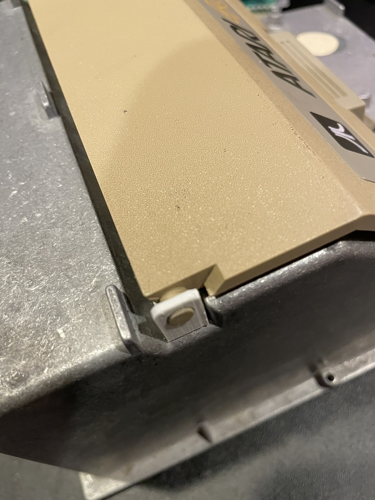
My collection of FujiNet hardware spanning the first ESP8266 unit to the pre-release version 1.6.


Saturday, February 29, 2020

Atari POKEY Actuation with Arduino

I've had floating in the back of my mind wanting to make a modern controller adapter for the Atari 5200. The 5200 controller is an analog joystick, two buttons, and a keypad. There are some modern controller projects that are really cool. As far as I can tell, they use digitally-controlled resistors to actuate the potentiometer inputs on the POKEY chip. Makes sense because that's what they were designed for - reading resistors.

The POKEY, along with a few external components, basically measures the time constant of an RC circuit. The system has an 1800-ohm resistor and 0.047 uF capacitor internal and the controller or paddle has a 0.5-1 M-ohm potentiometer. This makes for time constants ranging from <100 us to >10 ms. The operation is described in section 4 of the POKEY datasheet. The RC circuit can be seen in this excerpt of the 5200 schematic. The components on P0 (pin 14) are labeled.

The inputs P0-P7 are fed to Schmidt trigger inverters, which will go from high-to-low when the capacitor voltage reaches about 2 volts. The time that takes is determined by the resistance of the potentiometer. In otherwords, the time it takes to charge up the capacitor is measured by the POKEY.

Another way to charge the capacitor is to send in pulses of current (charge) over some time. I wondered if I could use the pulse width modulation (PWM) feature on modern microcontrollers, like the Atmega 328p used in the Arduino, to control how fast the capacitor charges. I had limited success. It turns out the PWM resolution required is much too fine. I would have to resort to additional timers and interrupts to fiddle with the PWM duty cycle and frequency.

Timers. Time. Hmmm. Charge up the capacitor at the right time!

Inside the POKEY is also a "dump transistor" that discharges the capacitor to reset the circuit for the next frame and reading. This is done by hitting the POTGO line. It can be seen in this schematic, again from the datasheet:
It's easy to charge up the capacitor - just apply some voltage for a few 10's of microseconds. But how to know when to do it? The dump transistors will pull the input pin to ground. If I monitor the paddle inputs and watch for it to go low, I know when the capacitors are reset and can start counting. Then I can send the input high at just the right time to trigger the POKEY.

This is super simple. And I made it work in a straightforward proof-of-concept. Here's the circuit:

The diode stops output PIN 3 from pulling down input on PIN 2. I want the dump transistor inside the POKEY to do the pulling. The proof-of-concept code is just some level checking and delays. This code can be used to reliably create readings from 1 to 227. Code 228 is made by just doing nothing, although to transition between 227 and 228 could be jittery because of the code trying to sync back up with the POTGO signal. A software PLL might be a way forward.

#include <Arduino.h>

void setup()
{
  pinMode(3, OUTPUT);
  pinMode(2, INPUT);

  // try to charge up the POT capacitor until it takes
  while (digitalRead(2) == LOW)
  {
    digitalWrite(3, HIGH);
    delayMicroseconds(64);
    digitalWrite(3, LOW);
  }

  // wait until dump transistor is activated
  while (digitalRead(2) == HIGH)
  {
  }
}

void loop()
{
  //trial and error on logic analyzer to get PADDLE(0)=1 despite a second late pulse
  delayMicroseconds(2190); // count up until dump transisstor is released
  delayMicroseconds(6350*2); // delay 100 line groups
  delayMicroseconds(636*2+63*5); // delay 10 & 1 line groups

  // charge up POT capacitor
  digitalWrite(3, HIGH);
  delayMicroseconds(63);
  digitalWrite(3, LOW);

   // wait until dump transistor clears cap with some debounce
  while (digitalRead(2) == HIGH)
  {
  }
  while (digitalRead(2) == HIGH)
  {
  }
}


Monday, November 25, 2019

Combo SIO2Arduino and RVERTER WiFi Modem for Atari 8-bits

I decided to glom Whizzosoft's SIO2Arduino and Paul Rickards' wifi modem together into a single ESP8266. It boots a single ATR file stored in SPIFFS. I demoed SIO2Arduino in a previous post.

Here's a video of it in action.


The code is on my GitHub.

Since doing this, I've joined the FujiNet development team to make something cooler.

Sunday, November 17, 2019

Atari on Papilio DUO

A few years ago I bought myself a Papilio DUO FPGA board. I was attracted to its Adruino Mega form factor and inclusion of an AVR Atmega32U4 chip. The IDE was based on the Arduino IDE. How cool - learn FPGAs inside what looked like the Arduino ecosystem. It also came with different shields - I bought the compute shield because it had joystick ports. Joystick ports. Did I say joystick ports? 

I ran through some demos and then set it aside. A year ago I started using is a logic analyzer for my Atari cartridge interface project. Recently, I decided to finally load up the Atari800 core I'd read about. I didn't do much research when I bought the board in 2015. Had I understood more, I probably would have bought a MIST, although the Papilio was about half the price I imagine. But I digress.


Thankfully, 64KiB.com (aka foft) ported the Atari FPGA implementation to the Papilio DUO. It loaded just fine, but it acted like the down arrow on the keyboard was stuck. Fortunately, the Papilio and 64KiB creators had already solved this problem.The AVR needed to be programmed for high-impedance inputs on all GPIOs. Whew. 

[NOTE: the website for the FPGA cores has moved to http://www.64kib.com/]

Another problem I ran into is keyboard mapping. I have a US-layout PS2 keyboard, which has a different layout of where the Atari arrow keys go compared to a UK-layout. I could only make the Atari cursor go in 3 directions. So RTFM and I learned about the UK-layout problem and started randomly trying CTRL-key combos. "CTRL-\" worked for me.

I played my GRAVITEN game, which was the second I wrote for the BASIC game competition. Fun.

Friday, June 14, 2019

Good Timing

In my last retrochallenge post I reported difficulty latching the address bus. Using the logic analyzer, I saw the latch signal was coming a but too late relative to the hold time of the address bus. I needed a way to edge trigger a shorter pulse. I found this handy circuit which creates a positive edge triggered pulse.

The pulse width is set by the RC time constant. I selected the resistor value to limit the current being sourced and sunk by the NAND gate (configured as an inverter). A value of 390 ohms limits the current to 13 mA peak, which is a 50% derating on the 25 mA absolute max allowed value for a LS74HCT00 device. The current spikes are short as they charge/discharge a small capacitor of a couple hundred pF to set the pulse width to 140 ns. I picked the cap somewhat by trial and error. The resulting timing looks like this:

The LE_D signal triggers the pulse generator, which outputs LE_A. The LE_A signal successfully latches the address before it changes right after the falling edge of phi2. 

Fortunately, I was able to use spare NAND and AND gates and only had to add the two passives. Almost free! Being able to latch the address allows the Atari handler and MCU software to be written to use a command/data protocol. The address specifies the command and the data shows up on the bus. I wonder what is possible with such an interface.

Friday, April 5, 2019

Retrochallenge 0319 - Last Post

I had to take a week off of the Retrochallenge to take care of life. I finished the month by making a completed circuit on a breadboard with mostly neat wires. I ran into trouble reading the address bus. The timing is too tight, so I need to change the latch signal for the address buffer.

The Retrochallenge is a good excuse to make some progress and to share the useless tinkering of the hobby. Here's what I have to show for it:

Thanks for following along!

Friday, March 22, 2019

The Flip Flop

I'm flip flopping like a politician on the data read algorithm in the Atmega328P MCU interface to the cartridge port. As described in previous posts, I was using an edge-triggered interrupt to alert the MCU that new data was ready. I chose the interrupt method because the original design was implemented on a single ESP32 that handled both the cartridge and wifi interfaces. The handling of the two interfaces was inherently asynchronous because they were both reacting to their external counterparts. The cartridge side didn't know when the Atari would push data and likewise with wifi and remote server. This didn't work very well given my rudimentary MCU programming skills. Splitting the system into two MCU's fixed the problem. It also allows a flip-flop to be made.

Researching this project, I ran across a website from Poland (that I can't find now) on interfacing to the 6502 bus. They used an SR flip-flop to latch the write enable signal before sending it to an MCU. The MCU could then poll the signal for a state change. While the interrupt method allows for simpler decoding logic, the polling makes for simpler software. And it's faster. The interrupt takes about 3 microseconds (several 6502 clock cycles). The polling can respond in half a microsecond or about a single 6502 cycle. This will add up to many saved clock cycles on the Atari side in the end.

Here's the concept.

The LE line goes low when the 6502 performs a STA $D5xx (described in this RC2019/03 post). The LE signal SETS the SR flip flop and its output Q tells the MCU it's time to read the data and address. The read operation is described here. Note, now the time between the LE going high and the /OEDATA going low is < 1 microsecond. It used to be 3 microseconds. Then the MCU sends a RESET to the SR flip flop and goes on to its next operation ...

... which is what I'm going to do, too.